Abstract

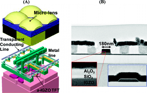
The integration of electronically active oxide components onto silicon circuits represents an innovative approach to improving the functionality of novel devices. Like most semiconductor devices, complementary-metal-oxide-semiconductor image sensors (CISs) have physical limitations when progressively scaled down to extremely small dimensions. In this paper, we propose a novel hybrid CIS architecture that is based on the combination of nanometer-scale amorphous In−Ga−Zn−O (a-IGZO) thin-film transistors (TFTs) and a conventional Si photo diode (PD). With this approach, we aim to overcome the loss of quantum efficiency and image quality due to the continuous miniaturization of PDs. Specifically, the a-IGZO TFT with 180 nm gate length is probed to exhibit remarkable performance including low 1/f noise and high output gain, despite fabrication temperatures as low as 200 °C. In particular, excellent device performance is achieved using a double-layer gate dielectric (Al2O3/SiO2) combined with a trapezoidal active region formed by a tailored etching process. A self-aligned top gate structure is adopted to ensure low parasitic capacitance. Lastly, three-dimensional (3D) process simulation tools are employed to optimize the four-pixel CIS structure. The results demonstrate how our stacked hybrid device could be the starting point for new device strategies in image sensor architectures. Furthermore, we expect the proposed approach to be applicable to a wide range of micro- and nanoelectronic devices and systems.
/files/info/2011/am1009088.pdf
