Single-shot readout of an electron spin in silicon
- Nature
- Volume:
- 467 ,
- Pages:
- 687–691
- Date published:
- (07 October 2010)
- DOI:
- doi:10.1038/nature09392
- Received
- Accepted
- Published online
The size of silicon transistors used in microelectronic devices is shrinking to the level at which quantum effects become important1. Although this presents a significant challenge for the further scaling of microprocessors, it provides the potential for radical innovations in the form of spin-based quantum computers2, 3, 4 and spintronic devices5. An electron spin in silicon can represent a well-isolated quantum bit with long coherence times6 because of the weak spin–orbit coupling7 and the possibility of eliminating nuclear spins from the bulk crystal8. However, the control of single electrons in silicon has proved challenging, and so far the observation and manipulation of a single spin has been impossible. Here we report the demonstration of single-shot, time-resolved readout of an electron spin in silicon. This has been performed in a device consisting of implanted phosphorus donors9 coupled to a metal-oxide-semiconductor single-electron transistor10, 11—compatible with current microelectronic technology. We observed a spin lifetime of ~6 seconds at a magnetic field of 1.5 tesla, and achieved a spin readout fidelity better than 90 per cent. High-fidelity single-shot spin readout in silicon opens the way to the development of a new generation of quantum computing and spintronic devices, built using the most important material in the semiconductor industry.
Figure 1: Spin readout device configuration and charge transitions.
a, Diagram showing the spin-dependent tunnelling configuration, where a single electron can tunnel onto the island of a SET only when in a spin-up state. b, Pulsing sequence for single-shot spin readout (see main text), and SET response, ISET. The dashed peak in ISET is the expected signal from a spin-up electron. The diagrams at the top depict the electrochemical potentials of the electron site (μ↓,↑), of the SET island (μSET) and of the drain contact (μD). c, Scanning electron micrograph of a device similar to the one measured. The area where the P donors are implanted is marked by the dashed square. Both d.c. voltages and pulses are applied to the gates as indicated. The red shaded area represents the electron layer induced by the top gate and confined beneath the SiO2 gate oxide layer. d, SET current ISET as a function of the voltages on the top and the plunger gates, Vtop and Vpl, at B = 0. The lines of SET Coulomb peaks are broken by charge transfer events. The blue arrow on the transition at Vpl ≈ −1.4 V shows the axis along which Vtop and Vpl are pulsed for compensated time-resolved measurements, ensuring that μSET remains constant during the pulsing. e, Line traces of ISET along the solid and dashed lines in d. Ionizing the donor shifts the sequence of SET current peaks by an amount ΔVtop = Δq/Ctop, causing a change ΔI in the current. The charging energy of the SET is ~1.5 meV.
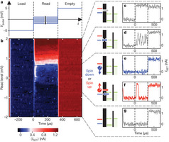
Figure 2: Single-shot spin readout and calibration of the ‘read’ level.
a, Three-level pulsing sequence for spin readout. The ‘load’ and ‘empty’ levels are kept constant, while the read level is scanned
 from high to low. b, SET current
  ISET
ISET , averaged over 128 single-shot traces (colour scale), as a function of the Vpulse level during the read phase. Data taken with an applied magnetic field B = 5 T and a detection bandwidth of 40 kHz (rise time ~10 μs). c–g, Examples of single-shot traces. c, Read level too high, μ↓ > μSET: the electron always leaves the donor during the read pulse, regardless of its spin. d, μ↓ ≈ μSET: random telegraph signal indicates an electron switching between SET island and |↓
 state. e, f, Correct read level, μ↓ < μSET < μ↑: ISET = 0 during the read phase indicates a |↓
 state (e). A single current pulse at the beginning of the read phase is the signature of a |↑
 state (f). The regime of correct read level is recognizable by the isolated increase in
  ISET
ISET in b. g, Read level too low, μ↑ < μSET: the electron never leaves the donor during the read pulse.
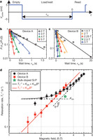
 Figure 3: Spin relaxation rate.
a, Pulsing sequence for measuring the spin relaxation rate 1/T1, identical to Fig. 1b but with a variable load/wait time, τw. b, c, Exponential decays of the normalized spin-up fraction at different magnetic fields, for devices A and B as indicated. d, Magnetic field dependence of T1−1. Error bars, 95% confidence levels. The data for device A follow T1−1 = 1.84 s−1 + 0.0076B5 s−1 T−5 (black solid line, sum of the dashed lines). The point at B = 1.75 T is not included in the fitted data set. The data for device B follow T1−1 = 0.015B5 s−1 T−5 (red line). The star is a data point measured on a bulk Si:P crystal at T < 5 K (J. J. L. Morton, personal communication).
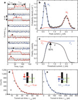
 Figure 4: Readout fidelity and visibility.
a, Examples of single-shot ISET traces, each shifted by 4 nA for clarity, with B = 5 T and 120 kHz bandwidth (~3 μs rise/fall time). The spin is labelled |↑
 (red trace) or |↓
 (blue trace), depending on whether ISET passes the threshold IT = 1.1 nA (dashed lines). b, Histogram (circles) of the maximum values of ISET in the interval 0 < t < 100 μs (black squares in a), obtained from a 10,000-shots data set. The blue and red lines are simulated histograms for states |↓
 and |↑
 , respectively, and the black dashed line is the sum of the two. The simulated curves are obtained using P↑ = 0.47, ΔI = 1.9 nA, 1/Γ↑,out = 10 μs, 1/Γ↓,in = 40 μs. c, |↓
 (blue) and |↑
 (red) readout fidelities, and readout visibility (black) as a function of the discrimination threshold, IT. The maximum visibility is 92% at IT ≈ 1.1 nA. d, e, Histogram (circles) of the tunnel-out times for spin-up electrons, τ↑,out (d), and subsequent tunnel-in times for spin-down electrons, τ↓,in (e), as defined on the top trace in a. In d, we note a systematic ~10 μs delay between the beginning of the read phase and the tunnel-out events, due to the response of the amplifier and filter chain. The solid lines are exponential fits to extract the tunnel rates. These values of 1/Γ↑,out and 1/Γ↓,in were used to obtain the simulated curves in b.
.jpg)
.jpg) tic broadening of electron states in the SET island. Therefore we perform the experiment in high magnetic fields, B
tic broadening of electron states in the SET island. Therefore we perform the experiment in high magnetic fields, B