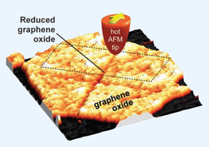
US researchers have 'drawn' tiny conductive lines on an insulating graphene oxide surface using the heated tip of an atomic force microscope that changes the local chemistry of the surface.
Graphene is of great interest for nanoelectronics because it is highly conductive, and is formed of a sheet of carbon atoms only one atom thick. It has potential for use in flat electronic applications such as mobile phones or smaller computers.
Graphene conducts very well, but it has proved difficult to find a way to reproducibly form graphene nanostructures of a particular shape and size, so they could be used in nanocircuitry, for example. A team of scientists led by Elisa Riedo at Georgia Institute of Technology and Paul Sheehan at the US Naval Research laboratory has now turned the problem on its head.
Instead of starting with graphene they take graphene oxide (GO), which is similar to graphene but does not conduct electricity. They use a technique they call thermochemical nanolithography (TCNL) to write on a GO surface with a heated scanning probe tip, just like writing on a sheet of paper with a pen. The warmed tip causes heating in a very specific point on the surface of the GO, and the heat alters the chemistry of the material just around the probe tip, making it conductive like graphene.

The hot atomic force microscope tip can be used to 'draw' conductive lines in graphene oxide
© Science
|
This conversion can be done controllably and quickly in just a single step, and the width of the lines drawn can range between 12 nanometres and 20 micrometres. Riedo says that 'the same tip used for writing can also be used to read it, which is very important for quality control' and hard to do quickly using existing methods.
Andre Geim, a physicist at University of Manchester, UK, known for the discovery of graphene, is surprised that such narrow nanoribbons can be created using the probe tip because heat travels so quickly in graphene that it would be like trying to paint a thin line with a thick brush. He adds that 'there is a general idea that using graphene sheets you can define features on an atomic level. This resolution is not yet enough but it is going in the right direction.'
The team now hopes that arrays of many, variably heated tips can be used simultaneously on a single surface to produce real nanosized circuits containing different functional parts.
Carol Stainer
Interesting? Spread the word using the 'tools' menu on the left.


